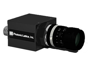
About Photonic Crystals
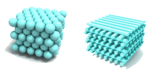
Photonic crystals are artificial structures made in regular patterns, a technology that enables control of light that cannot be achieved with naturally occurring materials. However, because of the need to precisely fabricate very fine structures, few companies have even put this technology to practical use.
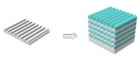
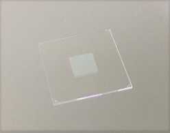
We have the technology to create photonic crystals simply by stacking multiple layers of films on a wafer with uneven surfaces.
The size of the unevenness can be freely varied from tens of nm to several micrometers.
We can create precise three-dimensional structures with a simple process of a single patterning and deposition of the films.
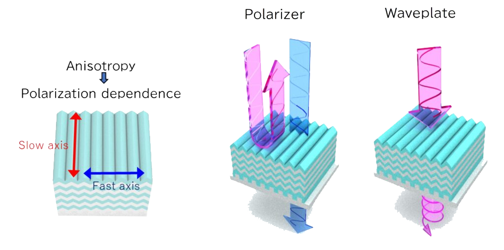
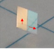
For example, in the structure shown on the right figure, anisotropy in the structure causes a difference in optical properties between vertical and horizontal polarization. The direction of anisotropy is determined by the pattern of the wafer.
When the thickness of each layer is controlled, the interference of light in the multilayer film allows it to function as a polarizer, in which one polarization is reflected, or as a waveplate, in which the polarization state is changed.
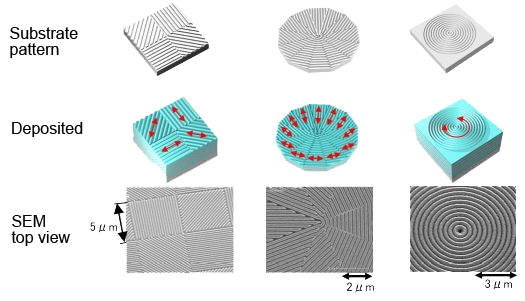
By changing the pattern of the wafer, polarizers and waveplates with various axial distributions can be freely made. In other words, free polarization distribution can be realized.
This technology is used in polarization imaging sensors, multichannel polarization conversion elements for optical communications, and as special filters for semiconductor wafer inspection.
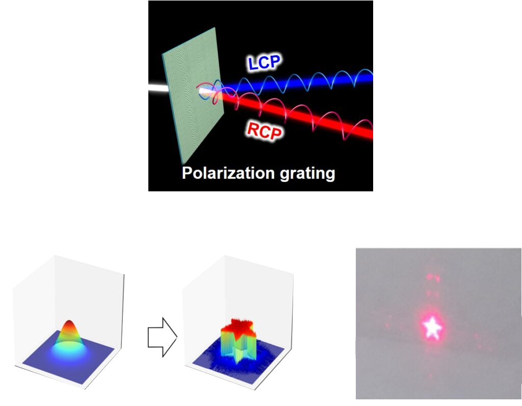
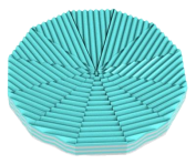
More recently, we have introduced the concept of geometric phase and are working to realize new functions through phase control. We have realized diffraction gratings that can separate left and right circular polarization and control beam shape.
The control of not only polarization but also phase is developing new applications.