WE AT PHOTONIC LATTICE REBIRTH IN 2022
“Focused on light, from our roots to the world”


Photonic Lattice, Inc. steps up in 2022
We, Photonic Lattice, Inc., inherited the optical measurement business of Photron Limited, our parent company since April 1, 2022. We will keep pursuing the evermore growing potential of light in all its form in various fields and will step up as a company providing global services to our partners.
“Great optical technologies, great quality”
In a sincere spirit of mutual respect and passion for technology,
we will keep contributing to society by providing unique optical solutions to our partners all over the world.
Thank you for your support and let’s go forward together.
HISTORY
Looking back on our trajectory from the origin of photonic crystals to our 20th anniversary,
we present the elements and minds that made us, as “a company focused on light.”
The origin of photic crystals
The term “photonic crystal” is a generic word referring to micro-structures exhibiting spatial periodicity in its refractive index. Surprisingly, while being a simple concept, it has begun to be used only recently, starting with an academic paper by the American physicist E. Yablonovitch in 1987. Initially proposed as high-density optical integrated circuits for perfect light confinement and high-efficiency lasers, they always were a big challenge to design and manufacture. With the development of the optical information society, this technology started to shine as a gemstone, by all the new possibilities it offers to the engineers in a growing number of fields.
1997
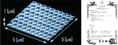
“Auto-cloning” process, our core technology, was developed as a reliable and efficient way of manufacturing photonic crystals, at Kawakami Laboratory, Research Institute of Electrical Communication, Tohoku University.
東北大学電気通信研究所川上研究室にて、当社のコア技術である「自己クローニング法によるフォトニック結晶作製技術」が発明されました。
2002
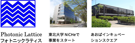
Photonic Lattice, Inc. was established.
The Company’s preparations started at NICHe of Tohoku university, before moving to new headquarters soon.
2003
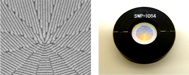
Starting development and sales of photonic crystal polarizers
Photonic crystals polarizers can, unlike conventional polarizers, exhibit non-uniform local properties, allowing to control accurately the state of polarization over its surface. Thus, they are can be tailored to any custom application requiring those properties. Furthermore, it is easy to design, prototype and manufacture. In various applications, ranging from laser technology to biotechnology and optical communication, we started releasing products including polarizers and retarder elements.
2006
Release of the PI-100 polarization camera
A camera that can ”see the polarization”, the first featuring photonic crystal-in the world.
2007
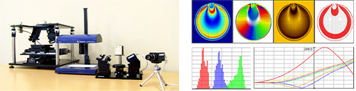
Release of the birefringence measurement system PA-100
Unlike point measurement type devices that were common at the time, our new system could acquire tens of thousands of data points within a few seconds. It drastically expanded the field of applications of birefringence measurement, including for example the evaluation of residual stress in resin molded products, like plastic lenses, and the inspection of transparent films. Based on the same polarization measurement technique, we also released the first version of a new-type ellipsometer, suitable for the thickness measurement of ultra-thin films, typically in the semiconductor industry.
2008
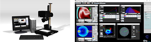
Release of the birefringence measurement system WPA-100
Improving dramatically the measurement range of previous PA-100, WPA-100 defied conventional wisdom at the time and continues to satisfy our customers now, through the periodic release of upgraded systems and additional features, such as the “Ultra-high retardation mode”, designed to satisfy ever growing markets needs.
2009
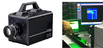
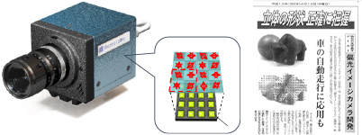
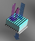
Start joint development with Photron
We succeeded at developing a high-speed polarization imaging sensor and released the world’s first high-speed polarization camera. With this technology, we contribute at elucidating phenomena that could not be visualized in the past, such as stress analysis in colliding elements in crash tests or the real-time spatial visualization of sound in the field of acoustics.
2010
Release of the high-speed mapping ellipsometer ME-110
By providing high-resolution and high-speed 2D evaluation of resist film on silicon wafers and organic film on transparent substrates, ME-100 and its successors expanded the polarization measurement applications to the semiconductor and display device industries. After that, we achieved further penetration into the mass-production segment by introducing auto-loader systems to the product.
2011
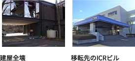
Facilities damaged by the Great East Japan earthquake
Although our building was irremediably damaged, most of the equipment was miraculously spared from destruction, allowing the company to quickly restart at a new location.
2011
Achieved 2M$ sales
2012
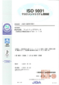
Acquired ISO9001 certification
Strengthened organization as a manufacturing company
製造業としての基礎を固めました。
2013
Achieved 100 units sales
2014
Started sales of optical communication elements in the United States
Mainly in the United States, we started new business of elements designed for optical coherent communication and wavelength selective switches. We then expanded our sales area to East Asia, in a context of rapid expansion of optical communication networks throughout the continent.
2015
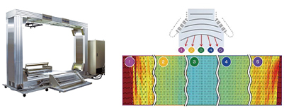
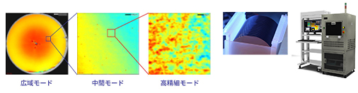
Released optical film inspection system KAMAKIRI
In order to meet the requirements for full-scale inspection of optical films used is flat display technologies, we released the world’s first full-length, full-width polarization inspection system, KAMAKIRI. We keep promoting and upgrading automatic inspection technologies solving the manufacturing and inspection issues faced by our partners.
2017
Acquired ISO 14001 certification
Further awareness of social contribution
and natural environment
Achieved 300 units sales
2019
Achieved 4M$ sales
Overseas sales exceed domestic sales for the first time
2020
Sales of photonic crystal polarization elements alone exceeded 1M$
The optical communication market in the United States and East Asia steadily growing up, we started developing new applications in such fields as laser processing and semiconductor inspection devices.
Achieved 400 units sales
2021
Joined Photron Group
While consolidating ever more our long-lasting collaboration
we started activities aiming at expanding our global business in Europe and the United States by developing new services and products.
2021
Became a consolidated group company of IMAGICA GROUP
2022.4
Logotype renewal
Business transfer and integration with Photron
We will keep pursuing greater optical technologies, always creating new value in a spirit of co-creation and mutual respect, by providing various products and services from our local roots in Sendai, Japan, to our global partner throughout the world. The integration with Photron’s optical measurement business will make possible the creation of an even more valuable and comprehensive service system, covering needs ranging from the design, prototyping and manufacture of optical elements, to system maintenance and sales, in order to answer flexibly and promptly to the ever-changing needs of our partners. Furthermore, by enhancing cooperation with Photron, we will be able to start new services in Europe and the United States, in addition to our historic markets in Japan and East Asia.
“Great optical technologies, great quality”
As a company focused on light, we promise to continue to provide unique optical solutions at a quality exceeding the expectations of our customers around the world, in a sincere spirit of co-creation, mutual respect, and passion for optical technologies.
PHOTONIC LATTICE