


最高の光学コンテンツを最高の品質とともに
We will continue to move forward with a sincere spirit and passion so that we can contribute to people
all over the world with our one-of-a-kind optical solutions.


TECHNOLOGY
よりよい情報社会と安全安心な社会を支える
最先端の光学素子と光学計測技術


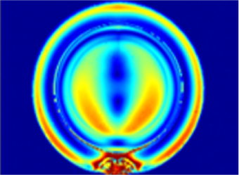
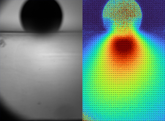
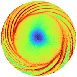
当社のコア技術は、様々な軸をもつマイクロ偏光素子アレイを1枚の基板上に自由なパタンでスパッタ技術によって積層するフォトニック結晶技術です。この技術は光通信(偏波多重)、半導体(DUV光による検査)、精密加工(ビーム整形)などにおける中核部品として、各分野の最先端装置に搭載されています。
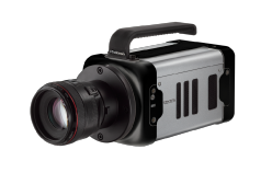
現在では、応用技術として特殊光学系や計算アルゴリズムを研究開発することによって、独自の複屈折計測装置、偏光高速度カメラ、超高速高感度サーモグラフィ、そして二酸化炭素イメージング装置などの独自製品を実現し、従来困難であった現象の可視化や計測を実現しています。
世界最小のモノサシとして普遍的な価値をもつ光の制御技術や利用シーンをとことん追求することによって、よりよい光情報社会や安全安心社会の実現に貢献してまいります。
SOLUTION
ソリューション
顧客の抱える問題やニーズに深く耳を傾け、それらの解決および最適な運用実現のための最先端光技術ソリューションを提案しています。
光学設計から製造まで一貫したモノづくり体制と、紫外から赤外波長まで広範に対応した素子やカメラを組みあわせることによって、顧客の期待を上回る問題解決法や価値創出を目指しています。


SOLUTION
PRODUCT
製品
独自の光学技術を用いた光学素子、光学モジュール、検査装置、特注開発、受託サービスを提供しています。
光学計測の精度や速度向上、未知現象の可視化や定量化にお困りの際は是非お問合せください。
PRODUCT
TECHNICAL
INFORMATION
お役立ち情報
光計測分野はまだまだ発展途上で、十分なノウハウや情報の共有がされていないという課題があります。
光でお困りのお客様にちょっと役立つ情報提供や情報交流を目指しています。
コラム
NEWS
お知らせ